


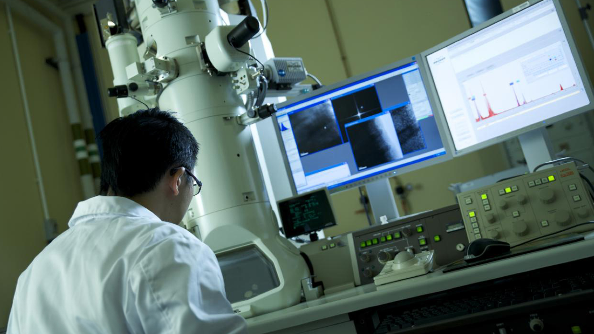

HKUST Researchers Develop a Novel Integration Scheme for Efficient Coupling Between III-V and Silicon
Researchers at the Hong Kong University of Science and Technology (HKUST) has recently developed a novel integration scheme for efficient coupling between III-V compound semiconductor devices and silicon components on silicon photonics (Si-photonics) platform by selective direct epitaxy1, unlocking the potential of integrating energy-efficient photonics with cost-effective electronics, as well as enabling the next generation telecommunications with low cost, high speed and large capacity.
Over the past few years, data traffic has been growing exponentially driven by various applications and emerging techniques such as big data, automobiles, cloud applications and sensors. To address the issues, Si-photonics has been widely investigated as a core technology to enable, extend, and increase data transmission through energy-efficient, high-capacity and low-cost optical interconnects. While silicon-based passive components have been well established on Si-photonics platform, the lasers and photodetectors can’t be realized by silicon and necessitate the integration of other materials such as III-V compound semiconductors on silicon.
III-V lasers and photodetectors on silicon has been investigated by two main methods. The first one is the bonding-based method which has yielded devices with impressive performance. However, it requires complicated manufacturing technique that is low yield and high-cost, making mass production very challenging. The other way is direct epitaxy method by growing multiple layers of III-V on silicon. While it provides a solution with lower cost, larger scalability and higher integration density, the micrometers thick III-V buffer layers which are crucial for this method hinders efficient light coupling between III-V and silicon - the key for integrated Si-photonics.
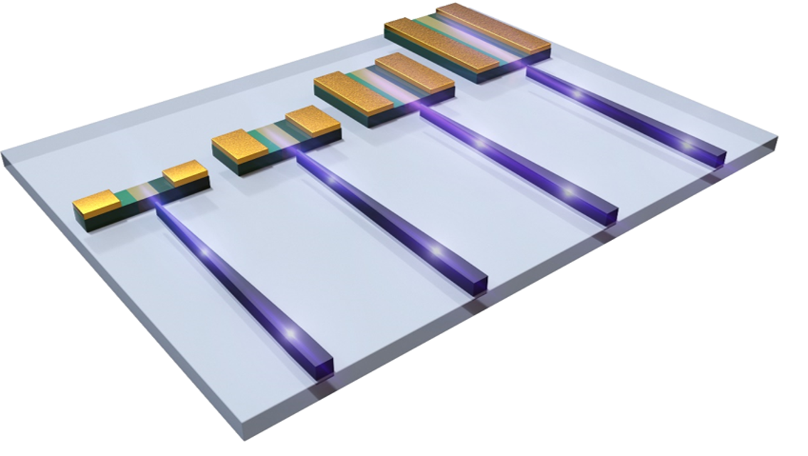
To address these issues, the team led by Prof. Kei-May LAU, Professor Emeritus of the Department of Electronic and Computer Engineering at Hong Kong University of Science and Technology (HKUST) developed lateral aspect ratio trapping (LART) - a novel selective direct epitaxy method that can selectively grow III-V materials on silicon-on-insulator (SOI) in a lateral direction without the need of thick buffers. Furthermore, based on this novel technology, the team devised and demonstrated unique in-plane integration of III-V photodetectors and silicon elements with high coupling efficiency between III-V and silicon. Compared to the commercial ones, the performance of photodetectors by such approach is less noisy, more sensitive, and has wider operation range, with record-high speed of over 112 Gb/s – way faster than existing products. For the first time, the III-V devices can be efficiently coupled with Si elements by direct epitaxy. The integration strategy can be easily applied to the integration of various III-V devices and Si-based components, thereby enabling the ultimate goal of integrating photonics with electronics on silicon photonics platform for data communications.
“This was made possible by our latest development of a novel growth technique named lateral aspect ratio trapping (LART) and our unique design of coupling strategy on the SOI platform. Our team’s combined expertise and insights into both device physics and growth mechanisms allow us to accomplish the challenging task of efficient coupling between III-V and Si and cross-correlated analysis of epitaxial growth and device performance,” said Prof. Lau.
“This work will provide practical solutions for photonic integrated circuits and fully integrated Si-photonics, light coupling between III-V lasers and Si components can be realized through this method” said Dr. Ying Xue, first author of the study.
This is a collaborative work with a research team led by Prof. Hon Ki Tsang of Department of Electronic Engineering at Chinese University of Hong Kong (CUHK) and a research team led by Prof. Xinlun Cai of School of Electronics and Information Technology at Sun Yat-sen University (SYSU). The device fabrication technology in the work was developed at HKUST’s Nanosystem Fabrication Facility (NFF) on Clear Water Bay campus. The work is supported by Research Grants Council of Hong Kong and Innovation Technology Fund of Hong Kong. This work has recently been published in Optica.
1Epitaxy is a technology used in the manufacturing process of semiconductor devices that grows new crystals on the original wafer to make new semiconductor layers.
Sign Up for Our Latest News
Latest News

Researchers from The Hong Kong University of Science and Technology (HKUST) have developed a novel chip architecture that enables the miniature acoustic devices inside smartphones to withstand over 12 times higher power loads while maintaining cooler and more stable operation.
Solar cells' efficiency and lifespan are often determined by what happens at interfaces — the microscopic boundaries where different materials meet. Researchers from The Hong Kong University of Science and Technology (HKUST) have contributed to two recently published studies that show molecular interface engineering can unlock major gains in the efficiency and durability of next-generation perovskite tandem solar cells.
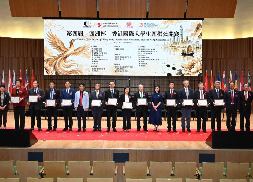
由香港大灣區圍棋促進會及香港科技大學(科大)聯合主辦的第四屆「四洲盃」香港國際大學生圍棋公開賽,於7月14日至18日在科大校園隆重舉行。賽事開幕典禮於今日(7月15日)在科大逸夫演藝中心盛大舉行,並非常榮幸邀請到香港特別行政區政府教育局局長蔡若蓮博士等重量級嘉賓蒞臨主禮。出席開幕儀式的嘉賓亦包括:香港大灣區圍棋促進會會長徐瑩女士、科大副校長(大學拓展)吳宏偉教授、四洲集團創辦人兼主席戴德豐博士、深圳市文化廣電旅遊體育局副局長何建輝先生、中央政府駐港聯絡辦宣傳文體部副部長林枬先生、外交部駐港特派員公署發言人兼新聞及公共關係部主任黃景睿先生、新華社亞太總分社社長孫承斌先生、中央廣播電視總台香港記者站站長王喜凱先生、中央廣播電視總台亞太總站副站長李風先生、先施集團主席、全國政協委員林曉暉先生、香港新聞工作者聯會會長張國良先生及科大跨學科學院院長屈華民教授等。